It has been described as an example of quantum physics in action, because to explain how it works, you need to talk about the energy levels of electrons within materials, in particular, semiconductor materials.
Three physicists, Bardeen, Brattain, and Shockley, developed the transistor (formed from the words "transconductance” and “varistor") and this was announced by the Bell Telephone Laboratories in 1948. Around the same time, German physicists Herbert Mataré and Heinrich Welker, at Westinghouse Laboratory in Paris also developed it. The Americans were later awarded the Nobel Prize for this work.
Semiconductors are substances that conduct electric currents, but only very poorly. They are in between true conductors (for example silver, aluminum, and copper) and non-conductors (examples are wool, cotton, paper, air, wood, and plastics). Two of the most commonly used semiconducting materials are the elements silicon and germanium. Important semiconducting compounds that have been developed include cadmium telluride, gallium arsenide and cadmium selenide.
Semiconducting materials fall into two categories: n-type and p-type semiconductors. n-type have a slight excess of electrons, while p-type have a deficiency of electrons (the deficiencies are known as holes). This why they are called bi-polar (holes and electrons).
Transistors consist of three layers, n-type/p-type/n-type (known as NPN) or p-type/n-type/p-type (known as PNP). The most commonly used transistors are NPN type, and they come in different shapes and sizes, but they usually have 3 legs, connectors to the three layers. The transistor shown below has a D-shaped cross section (it's lying on its flat surface) and E, B and C correspond to Emitter, Base and Collector - the 3 regions.The middle slice of the transistor is known as the base, and if the transistor is included in a circuit, so that current can flow through it, the current flows into the transistor through the collector, across the base, and out through the emitter.
This current can be controlled by applying a second source of electric current to the base. The amount of current that flows between the collector and emitter will be determined by the base current, so the collector emitter current will be switched off with no base current. With a relatively small base current, the collector emitter current is small, and if a relatively large current is allowed to flow into the base, the transistor allows a much larger flow of current through it. So the transistor acts like a switch and/or as an amplifier.
Below is an example of two identical NPN transistors, TR1 and TR2, working together. The input voltage causes a base current at TR1 which gives rise to a collector-emitter current (indicated by the direction of the arrow). This becomes the base current for TR2, and an even bigger collector-emitter current flows through TR2, making the pair very sensitive to changes in the INPUT voltage:
My example is a "darkness detector". It uses 2 NPN general purpose transistors (BC548B) arranged together in what's known as a Darlington Pair:
A nice animation for demonstrating it working was found on the following excellent site:
The transistors in the diagram above are drawn with (going clockwise) the Collector and Base in red, with the Emitter in grey:
The variable resistor is the component with a screw-head, for adjustment. The light dependent resistor (LDR) or photo-resistor is on the left and the moving object is blocking different amounts of light from reaching the LDR. The less light incident on the resistor, the more resistance it has (more than 20kΩ), and the more voltage there is across the LED. So when the ambient light's dark, the LDR has a resistance of around 1.5kΩ and the LED glows, when it's bright, the LED is off, and it is very sensitive for detecting the degree of darkness in between the two.
The circuit can also be built with a single transistor, but the Darlington Pair configuration makes the circuit much more sensitive to the small current changes produced by the incident light.
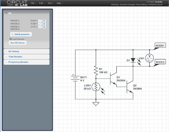
Circuit Lab (www.circuitlab.com) is excellent for designing and examining waveforms and voltages in circuit designs, before actually building the circuit. Have a look at the DC information in the left-hand panel below, giving information on the voltage between NODE1 and NODE2 ie across the LED.
I ran Circuit Lab on 2 cases - one where the LDR was illuminated (measured resistance ~9kΩ) and one where it was relatively un-illuminated (measured resistance ~20kΩ):
Above: AMBIENT LIGHT ON: V(Node1)-V(Node2) ie the voltage across the LED, [see the text in the upper left] is 319.9 mV - NOT enough to turn on the LED
Above: AMBIENT LIGHT OFF: V(Node1)-V(Node2) ie the voltage across the LED, [see the text in the upper left] is 2.575V - enough to turn on the LED.
Note that the transistors aren't the same model as mine, but generally, as long as they are also NPNs, it doesn't really matter.


No comments:
Post a Comment